USBtinyISP

Blown 74AHC125

I have the USBtinyISP kit from adafruit.com and I blew the 74AHC125 IC when I was working late at night and accidentally connected VCC (or perhaps RESET) with 12V VIN. Oops. I checked my cabinet for a replacement part but, alas, I didn’t have one. I figured I was out of commission with the USBtinyISP until realized what the 74AHC125 part was being used for – a level shifter. Since I am currently working in 5V only, I didn’t really need the level shifting feature so I decided to remove until I could order a some replacement 74AHC125’s. I didn’t have this part in a DIP socket so I first clipped the legs at the shoulder and began to de-solder the legs. When everything was cleaned up, I installed a DIP socket and then put jumpers in the slots between pins 2-3, 5-6, 8-9, and 11-12.

_MG_0752

This would turn out to work for until the replacement part came in fine except that reset would always be low since 2OE is ignored. To workaround this limitation, I would just remove the programmer to continue testing/debugging.

Update the firmware

Since I had the programmer apart, I decided to upgrade the firmware from 1.04 to 1.06. I also didn’t have a 12MHz crystal/resonator on hand so I improvised again. Using the resonator on the USBtinyISP I was able to update the firmware using my Arduino UNO as an avrisp.

_MG_0755

In the image you can see that I added jumper wire from pins 4, 5, and 10 of the ATtiny 2313 in the breadboard to the socket’s pins 4, 5, and 10 (respectively). Using this setup, I was able to upgrade the firmware and now I can use the USBtinyISP in a WinXP guest using VirtualBox and the setup described here.

Posted in Arduino, AVR, USBtinyISP

Realtek r8168 on Ubuntu 12.04

  1. Download the driver from here, current version is 8.038.00.
  2. Extract to /usr/src

    cd /usr/src
    tar xjvf ~/Downloads/r8168-8.038.00.tar.bz2
    
  3. Create /usr/src/r8168-8.038.00/dkms.conf

    PACKAGE_NAME="r8168"
    PACKAGE_VERSION="8.038.00"
    CLEAN[0]="make clean"
    BUILT_MODULE_NAME[0]="r8168"
    BUILT_MODULE_LOCATION[0]="src"
    DEST_MODULE_LOCATION[0]="/updates"
    MAKE[0]="'make' 'modules'"
    AUTOINSTALL="YES"
    REMAKE_INITRD="YES"
    

  4. Add, Build and Install the module with DKMS

    dkms add -m r8168 -v 8.038.00
    dkms build -m r8168 -v 8.038.00
    dkms install r8168/8.038.00
    

Tagged with: , , ,
Posted in Linux, Ubuntu

Adding SDRAM for Nios II on DE0-Nano

Introduction

Here I will be following up on the previous post and adding an SDRAM Controller and the IP Signals Core to the Nios II system on the DE0-Nano education board. The documentation I will be following can be found in the references section.

If not already done, you should install Altera’s University Program IP Cores which contains clock signal core IP to account for the -3ns phase shift to the 50MHz system clock to ensure correct timing for the SDRAM chip on the DE0-Nano [2].

Add SDRAM Controller and UP Clocks

Follow Section 5 in [1], read 6, and then continue to 7. The steps are very straight-forward but don’t forget to export clocks.sdram_clk as sdram_clk and sdram.wire as sdram_wire – see the Export column in Figure 12.

Update Top Level Module

module lights (
	input CLOCK_50,
	input [3:0] SW,
	input [0:0] KEY,
	output [7:0] LED,
	output DRAM_CLK,
	output DRAM_CKE,
	output [12:0] DRAM_ADDR,
	output [1:0] DRAM_BA,
	output DRAM_CS_N,
	output DRAM_CAS_N,
	output DRAM_RAS_N,
	output DRAM_WE_N,
	inout [15:0] DRAM_DQ,
	output [1:0] DRAM_DQM
);

nios_system NiosII (
        .clk_clk          (CLOCK_50),
        .reset_reset_n    (KEY),
        .switches_export  (SW),
        .leds_export      (LED),
		  .sdram_clk_clk    (DRAM_CLK),
		  .sdram_wire_cke   (DRAM_CKE),
		  .sdram_wire_addr  (DRAM_ADDR),
		  .sdram_wire_ba    (DRAM_BA),
		  .sdram_wire_cs_n  (DRAM_CS_N),
		  .sdram_wire_cas_n (DRAM_CAS_N),
		  .sdram_wire_ras_n (DRAM_RAS_N),
		  .sdram_wire_we_n  (DRAM_WE_N),
		  .sdram_wire_dq    (DRAM_DQ),
		  .sdram_wire_dqm   (DRAM_DQM)
    );

endmodule

Pin Assignments

There are a number of pin assignments required to setup the DRAM module so would suggest adding them through the Tcl console. Copy and paste the text from below or see the contents of the DE0-Nano.qsf file.

set_location_assignment PIN_P2 -to DRAM_ADDR[0]
set_location_assignment PIN_N5 -to DRAM_ADDR[1]
set_location_assignment PIN_N6 -to DRAM_ADDR[2]
set_location_assignment PIN_M8 -to DRAM_ADDR[3]
set_location_assignment PIN_P8 -to DRAM_ADDR[4]
set_location_assignment PIN_T7 -to DRAM_ADDR[5]
set_location_assignment PIN_N8 -to DRAM_ADDR[6]
set_location_assignment PIN_T6 -to DRAM_ADDR[7]
set_location_assignment PIN_R1 -to DRAM_ADDR[8]
set_location_assignment PIN_P1 -to DRAM_ADDR[9]
set_location_assignment PIN_N2 -to DRAM_ADDR[10]
set_location_assignment PIN_N1 -to DRAM_ADDR[11]
set_location_assignment PIN_L4 -to DRAM_ADDR[12]
set_location_assignment PIN_M7 -to DRAM_BA[0]
set_location_assignment PIN_M6 -to DRAM_BA[1]
set_location_assignment PIN_L7 -to DRAM_CKE
set_location_assignment PIN_R4 -to DRAM_CLK
set_location_assignment PIN_P6 -to DRAM_CS_N
set_location_assignment PIN_G2 -to DRAM_DQ[0]
set_location_assignment PIN_G1 -to DRAM_DQ[1]
set_location_assignment PIN_L8 -to DRAM_DQ[2]
set_location_assignment PIN_K5 -to DRAM_DQ[3]
set_location_assignment PIN_K2 -to DRAM_DQ[4]
set_location_assignment PIN_J2 -to DRAM_DQ[5]
set_location_assignment PIN_J1 -to DRAM_DQ[6]
set_location_assignment PIN_R7 -to DRAM_DQ[7]
set_location_assignment PIN_T4 -to DRAM_DQ[8]
set_location_assignment PIN_T2 -to DRAM_DQ[9]
set_location_assignment PIN_T3 -to DRAM_DQ[10]
set_location_assignment PIN_R3 -to DRAM_DQ[11]
set_location_assignment PIN_R5 -to DRAM_DQ[12]
set_location_assignment PIN_P3 -to DRAM_DQ[13]
set_location_assignment PIN_N3 -to DRAM_DQ[14]
set_location_assignment PIN_K1 -to DRAM_DQ[15]
set_location_assignment PIN_R6 -to DRAM_DQM[0]
set_location_assignment PIN_T5 -to DRAM_DQM[1]
set_location_assignment PIN_L1 -to DRAM_CAS_N
set_location_assignment PIN_L2 -to DRAM_RAS_N
set_location_assignment PIN_C2 -to DRAM_WE_N

set_instance_assignment -name IO_STANDARD "3.3-V LVTTL" -to DRAM_ADDR[0]
set_instance_assignment -name IO_STANDARD "3.3-V LVTTL" -to DRAM_ADDR[1]
set_instance_assignment -name IO_STANDARD "3.3-V LVTTL" -to DRAM_ADDR[2]
set_instance_assignment -name IO_STANDARD "3.3-V LVTTL" -to DRAM_ADDR[3]
set_instance_assignment -name IO_STANDARD "3.3-V LVTTL" -to DRAM_ADDR[4]
set_instance_assignment -name IO_STANDARD "3.3-V LVTTL" -to DRAM_ADDR[5]
set_instance_assignment -name IO_STANDARD "3.3-V LVTTL" -to DRAM_ADDR[6]
set_instance_assignment -name IO_STANDARD "3.3-V LVTTL" -to DRAM_ADDR[7]
set_instance_assignment -name IO_STANDARD "3.3-V LVTTL" -to DRAM_ADDR[8]
set_instance_assignment -name IO_STANDARD "3.3-V LVTTL" -to DRAM_ADDR[9]
set_instance_assignment -name IO_STANDARD "3.3-V LVTTL" -to DRAM_ADDR[10]
set_instance_assignment -name IO_STANDARD "3.3-V LVTTL" -to DRAM_ADDR[11]
set_instance_assignment -name IO_STANDARD "3.3-V LVTTL" -to DRAM_ADDR[12]
set_instance_assignment -name IO_STANDARD "3.3-V LVTTL" -to DRAM_BA[0]
set_instance_assignment -name IO_STANDARD "3.3-V LVTTL" -to DRAM_BA[1]
set_instance_assignment -name IO_STANDARD "3.3-V LVTTL" -to DRAM_CKE
set_instance_assignment -name IO_STANDARD "3.3-V LVTTL" -to DRAM_CLK
set_instance_assignment -name IO_STANDARD "3.3-V LVTTL" -to DRAM_CS_N
set_instance_assignment -name IO_STANDARD "3.3-V LVTTL" -to DRAM_DQ[0]
set_instance_assignment -name IO_STANDARD "3.3-V LVTTL" -to DRAM_DQ[1]
set_instance_assignment -name IO_STANDARD "3.3-V LVTTL" -to DRAM_DQ[2]
set_instance_assignment -name IO_STANDARD "3.3-V LVTTL" -to DRAM_DQ[3]
set_instance_assignment -name IO_STANDARD "3.3-V LVTTL" -to DRAM_DQ[4]
set_instance_assignment -name IO_STANDARD "3.3-V LVTTL" -to DRAM_DQ[5]
set_instance_assignment -name IO_STANDARD "3.3-V LVTTL" -to DRAM_DQ[6]
set_instance_assignment -name IO_STANDARD "3.3-V LVTTL" -to DRAM_DQ[7]
set_instance_assignment -name IO_STANDARD "3.3-V LVTTL" -to DRAM_DQ[8]
set_instance_assignment -name IO_STANDARD "3.3-V LVTTL" -to DRAM_DQ[9]
set_instance_assignment -name IO_STANDARD "3.3-V LVTTL" -to DRAM_DQ[10]
set_instance_assignment -name IO_STANDARD "3.3-V LVTTL" -to DRAM_DQ[11]
set_instance_assignment -name IO_STANDARD "3.3-V LVTTL" -to DRAM_DQ[12]
set_instance_assignment -name IO_STANDARD "3.3-V LVTTL" -to DRAM_DQ[13]
set_instance_assignment -name IO_STANDARD "3.3-V LVTTL" -to DRAM_DQ[14]
set_instance_assignment -name IO_STANDARD "3.3-V LVTTL" -to DRAM_DQ[15]
set_instance_assignment -name IO_STANDARD "3.3-V LVTTL" -to DRAM_DQM[0]
set_instance_assignment -name IO_STANDARD "3.3-V LVTTL" -to DRAM_DQM[1]
set_instance_assignment -name IO_STANDARD "3.3-V LVTTL" -to DRAM_CAS_N
set_instance_assignment -name IO_STANDARD "3.3-V LVTTL" -to DRAM_RAS_N
set_instance_assignment -name IO_STANDARD "3.3-V LVTTL" -to DRAM_WE_N

Testing the System

You should be able to re-generate the BSP from the project_name context sensitive menu (Nios II -> Generate BSP). However I had trouble with this and had to remove and re-add the projects.

References

Tagged with: , , ,
Posted in FPGA

Nios II on DE0-Nano

Introduction

For this I am using Quartus II Web Edition 13.0 SP1, which contains Qsys and Nios II EDS. I will initially follow the steps found in [1] up to section 7 where instead I will move to using Nios II Software Build Tools for Eclipse to build and deploy a test application.

System Creation

Create the project in Quartus II, start Qsys, and add the Nios II soft processor, as per [1]. The DE0-Nano, like the DE2-115, uses a 50MHz clock source. You are able to select and use theNios II/s and Nios II/f versions of the processor, however, unless you purchase a license, you will be presented with a dialog window after configuring the FPGA about the time limited OpenIP core. Do not close this window until you are finished or you will not be able to load any applications on the processor.

The remainder of the setup in Qsys is very straight-forward. You may realize that when adding the PIO core for the switches you used a width of 8 bits but the DE0-Nano only contains 4 switches. This is fine – I modified the width down to 4 bits and this did not affect the outcome of the base-end address range assigned by Qsys when using System->Assign Base Addresses (end = base + Fh).

As you prepare to instantiate the Nios II system, [1] suggests to call the parameter for the LEDs LEDG, however the DE0-Nano QSF uses the name LED. You should be able to account for this in Pin Planner but if you want to enter the assignments directly, say using the tcl console, then use the text below which uses LEDG.

set_location_assignment PIN_A15 -to LEDG[0]
set_location_assignment PIN_A13 -to LEDG[1]
set_location_assignment PIN_B13 -to LEDG[2]
set_location_assignment PIN_A11 -to LEDG[3]
set_location_assignment PIN_D1 -to LEDG[4]
set_location_assignment PIN_F3 -to LEDG[5]
set_location_assignment PIN_B1 -to LEDG[6]
set_location_assignment PIN_L3 -to LEDG[7]
set_instance_assignment -name IO_STANDARD "3.3-V LVTTL" -to LEDG[0]
set_instance_assignment -name IO_STANDARD "3.3-V LVTTL" -to LEDG[1]
set_instance_assignment -name IO_STANDARD "3.3-V LVTTL" -to LEDG[2]
set_instance_assignment -name IO_STANDARD "3.3-V LVTTL" -to LEDG[3]
set_instance_assignment -name IO_STANDARD "3.3-V LVTTL" -to LEDG[4]
set_instance_assignment -name IO_STANDARD "3.3-V LVTTL" -to LEDG[5]
set_instance_assignment -name IO_STANDARD "3.3-V LVTTL" -to LEDG[6]
set_instance_assignment -name IO_STANDARD "3.3-V LVTTL" -to LEDG[7]

Top Level Module

You can add the top level file to perform the system instantiation in either Verilog or VHDL as described in [1]. You can copy the Verilog code from the block below. Notice that the input SW is four bits instead of eight. This is because we only have four switches on the DE0-Nano.

module lights (
	input CLOCK_50,
	input [3:0] SW,
	input [0:0] KEY,
	output [7:0] LEDG
);

nios_system NiosII (
        .clk_clk         (CLOCK_50),
        .reset_reset_n   (KEY),
        .switches_export (SW),
        .leds_export     (LED)
    );

endmodule

Also add the .qip file which is generated by Qsys, Project->Add/Remove Files in Project. Browse for the .qip file using the … button in directory lights/synthesis (change the filer in the open file dialog to see IP Variation Files). Once selected, click the Add button and then OK to close the Settings window.
The inputs/outputs will be the physical pins to be setup in the next section.

Pin Assignments

With Pin Planner

First start Analysis & Elaboration (Processing -> Start -> Analysis & Elaboration) and then open the Pin Planner (Assignments -> Pin Planner). Then review the diagram below and make your window look similar.

pin_assignments

Manually

You can manually add the pin assignments using the Tcl console window (View -> Utility Windows -> Tcl Console). You may copy the assignments from the code blocks above (for LEDG) and below for KEY[0] and SW[3:0].

set_location_assignment PIN_J15 -to KEY[0]
set_instance_assignment -name IO_STANDARD "3.3-V LVTTL" -to KEY[0]
set_location_assignment PIN_M1 -to SW[0]
set_location_assignment PIN_T8 -to SW[1]
set_location_assignment PIN_B9 -to SW[2]
set_location_assignment PIN_M15 -to SW[3]
set_instance_assignment -name IO_STANDARD "3.3-V LVTTL" -to SW[0]
set_instance_assignment -name IO_STANDARD "3.3-V LVTTL" -to SW[1]
set_instance_assignment -name IO_STANDARD "3.3-V LVTTL" -to SW[2]
set_instance_assignment -name IO_STANDARD "3.3-V LVTTL" -to SW[3]

Timing

When running through the TimeQuest tutorial, [5], I found that I had to add CLOCK_50, set the clock uncertainty, and derive the clock uncertainty after reading the SDC file. All of this can be done through the Constraints menu; see the screen shots below to see what values I used.

CreateClock

SetClockUncertainty

DeriveClockUncertainty

Then update the timing netlist and report setup summary. When finished CLOCK_50 has 12.703ns slack, YMMV. Write the SDC file and add the output the project in Quartus II. Below are the relevant entries in the SDC file for CLOCK_50. You may also see similar lines for altera_reserved_tck and the setup of false paths.

create_clock -name {CLOCK_50} -period 20.000 -waveform { 0.000 10.000 } [get_ports {CLOCK_50}]
set_clock_uncertainty -rise_from [get_clocks {CLOCK_50}] -rise_to [get_clocks {CLOCK_50}]  0.020  
set_clock_uncertainty -rise_from [get_clocks {CLOCK_50}] -fall_to [get_clocks {CLOCK_50}]  0.020  
set_clock_uncertainty -fall_from [get_clocks {CLOCK_50}] -rise_to [get_clocks {CLOCK_50}]  0.020  
set_clock_uncertainty -fall_from [get_clocks {CLOCK_50}] -fall_to [get_clocks {CLOCK_50}]  0.020  

Configuring the FPGA

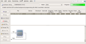
Start the Quartus II Programmer from Quartus II Tools->Programmer. The programmer may start with everything ready to go, if not follow these steps.

  • Press the Hardware Setup… button and select the USB-Blaster
  • Press the Auto Detect button
  • Highlight the row with the device EP4CE22CF17 and then Edit->Change File; browse for the .SOF file, check in the output_files folder
  • Ensure that Program/Configure is selected
  • Press the Start button

Programmer

Testing the System

Start Eclipse for Nios II (Tools->Nios II Software Build Tools for Eclipse). Create a new Nios II Application and BSP from Template. Browse for the SOPC file created by Qsys, the CPU name should be automatically selected. Enter your desired project name and select Blank Template as the Project template. Click the Finish button.

You now have two projects, project_name and project_name_bsp, select project_name, right-click and select new file, and enter a file name. Copy the contents of the block below into the new file and save. You can now run the project as a Nios II hardware and play with the switches to change which LEDs are illuminated.

#include <system.h>

#define switches (volatile char*)SWITCHES_BASE
#define leds (char*)LEDS_BASE

int main()
{
	while(1)
	{
		*leds = ((~(*switches) & 0x0F) << 4) | *switches;
	}
	return 0;
}

Follow-up

References

Tagged with: , , ,
Posted in FPGA